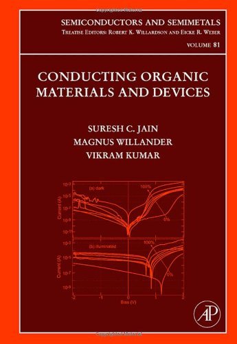
By Suresh C. Jain,M. Willander,V. Kumar
ISBN-10: 0127521909
ISBN-13: 9780127521909
Read or Download Conducting Organic Materials and Devices: 81 (Semiconductors and Semimetals) PDF
Best optical engineering books
New PDF release: Silicon Photonics: An Introduction
The transforming into call for for immediate and trustworthy communique signifies that photonic circuits are more and more discovering purposes in optical communications platforms. one of many major applicants to supply passable functionality at low-cost within the photonic circuit is silicon. when silicon photonics is much less good constructed compared to a couple different fabric applied sciences, it truly is poised to make a major effect at the telecommunications undefined, in addition to in lots of different purposes, as different applied sciences fail to fulfill the yield/performance/cost trade-offs.
The identify clarify new means of secured and excessive skill optical conversation signs iteration by utilizing the micro and nano ring resonators. The pulses are referred to as soliton pulses that are extra secured as a result of having the houses of chaotic and darkish soliton indications with extremely brief bandwidth.
New PDF release: Refined Ray Tracing inside Single- and Double-Curvatured
This booklet describes the ray tracing results within diversified quadric surfaces. Analytical floor modeling is a priori requirement for electromagnetic (EM) research over aerospace systems. even though numerically-specified surfaces or even non-uniform rational foundation spline (NURBS) can be utilized for modeling such surfaces, for many functional EM purposes, it's adequate to version them as quadric floor patches and the hybrids thereof.

This newest quantity of the well known Physics of skinny movies sequence contains 4 chapters that debate high-density plasma resources for fabrics processing, electron cyclotron resonance and its makes use of, unbalancedmagnetron sputtering, and particle formation in skinny movie processing plasma. bankruptcy One develops a unified framework from which all "high-efficiency" assets should be seen and in comparison; outlines key parts of resource layout affecting processing effects; and highlights parts the place extra study and improvement are neededChapter experiences and analyzes the most forms of electron cyclotron resonance (ECR) plasma resources compatible for ECR PACVD of skinny movies, frequently ECR resources utilizing magnet coilsChapter 3 examines the advantages and boundaries of the hot process, unbalanced magnetron sputtering (UBM), in addition to the inducement for its improvement, the fundamental ideas of its operation and advertisement functions, and a few speculations concerning the way forward for UBM technologyChapter 4 describes common phenomena saw in reference to particle formation in skinny movie processing plasmas; discusses debris in PECVD plasmas, sputtering plasmas, and RIE plasmas; provides an outline of the theoretical modeling of varied elements of debris in processing plasmas; examines problems with apparatus layout affecting particle formation; and concludes with comments in regards to the implications of this paintings for the regulate of process-induced particle illness
- Femtosekundenlaser: Einführung in die Technologie der ultrakurzen Lichtimpulse (German Edition)
- Advances in Electronic Testing: Challenges and Methodologies: 27 (Frontiers in Electronic Testing)
- Optics of Nanomaterials
- Subsea Optics and Imaging (Woodhead Publishing Series in Electronic and Optical Materials)
Extra resources for Conducting Organic Materials and Devices: 81 (Semiconductors and Semimetals)
Example text
Conducting Organic Materials and Devices: 81 (Semiconductors and Semimetals) by Suresh C. Jain,M. Willander,V. Kumar
by Michael
4.2